The Evolution of Microstrip Filter Technology
Microstrip filter technology was first released in 1952, and since then, numerous advancements in both dielectric material manufacturing and thin film processing techniques have led to the adoption of microstrip filtering for a wider range of applications, especially at mmWave frequencies.
Modern microstrip filters combine the advantages of planar fabrication with sophisticated electromagnetic design, enabling compact, low-cost filtering solutions for applications from mobile phones to satellite communications.
How Microstrip Filter Technology Works
Basic Principle
At a high level, microstrip refers to a type of planar transmission line technology that consists of a conducting strip separated from a ground plane by a dielectric substrate, as shown in Figure 1.
More specifically, the design and construction of a microstrip filter is similar to the way circuits are configured on a printed circuit board (PCB). However, a key distinction of a microstrip filter is that the metal conductor patterns printed on the solid dielectric substrate are there to create resonators rather than just interconnects.
Structure and Fields
The metal circuit patterns of strip elements are placed on a solid dielectric insulating layer with a metal ground layer below the dielectric. The fields surrounding the strip permeate two different media, with part of the field in the substrate and another in the air above the strip.
The higher permittivity of the dielectric substrate causes the electric field to concentrate in the substrate, which means field losses due to material choice become a factor. This makes the selection of substrate material critical for filter performance.
Substrate Materials for Microstrip Filters
Low-Frequency Applications (< 1 GHz)
FR4 Standard PCB Material
- Dielectric Constant (εᵣ): 4.3-4.7
- Loss Tangent (tan δ): 0.02
- Cost: Very Low
- Application: Commercial products, prototyping
Standard PCB materials like FR4 can be used below 1GHz for low-Q filters. While FR4 is inexpensive and readily available, its relatively high loss tangent limits performance in demanding applications.
Mid-Frequency Applications (1-10 GHz)
Rogers RO4003C
- Dielectric Constant: 3.38 ± 0.05
- Loss Tangent: 0.0027 @ 10GHz
- Cost: Medium
- Application: Wi-Fi, GPS, cellular
Rogers RO4350B
- Dielectric Constant: 3.48 ± 0.05
- Loss Tangent: 0.0037 @ 10GHz
- Cost: Medium
- Application: General-purpose RF
High-Frequency Applications (> 10 GHz)
Rogers RO3003
- Dielectric Constant: 3.00 ± 0.04
- Loss Tangent: 0.0010 @ 10GHz
- Cost: High
- Application: Millimeter-wave, satellite
Ceramic Materials
- Dielectric Constant: 2-10 (controlled)
- Loss Tangent: < 0.001
- Cost: Very High
- Application: High-performance filters
Lower loss and increased Q can be achieved using ceramic materials and specialized RF laminates, enabling filters with sharper roll-off and lower insertion loss.
Advantages of Microstrip Filters
This type of printed transmission line is a popular filtering option for several reasons:
1. Broad Frequency Coverage
Microstrip filters can cover a broad frequency range from UHF (300 MHz) to millimeter-wave (60+ GHz) frequencies, making them versatile for many applications.
2. Economical Production
- No Special Tooling - Uses standard PCB manufacturing processes
- Batch Fabrication - Multiple units produced simultaneously
- High Yield - Automated manufacturing ensures consistency
- Low Setup Cost - Design changes don’t require expensive retooling
3. Compact and Lightweight
Microstrip filters are often lighter and more compact than alternative transmission line technologies such as waveguide or coaxial cavity filters, making them ideal for:
- Mobile devices
- Aircraft and satellite systems
- Portable equipment
- Space-constrained applications
4. Easy Integration
- Direct PCB Integration - Filters built directly on system PCB
- No Connectors - Eliminates connector losses and failures
- Flexible Routing - Transmission line bends accommodate layout constraints
- Multiple Filters - Several filters on single substrate
Overcoming Loss Challenges
The Loss Problem
The biggest concern with microstrip filters is the loss experienced compared with other transmission-line and waveguide filtering approaches. Losses in microstrip filters come from several sources:
1. Conductor Losses
- Surface roughness increases resistance
- Skin effect at high frequencies
- Thin metallization (typically 17-35 μm copper)
2. Dielectric Losses
- Energy dissipated in substrate
- Increases with frequency and tan δ
- Temperature dependent
3. Radiation Losses
- Open structure allows electromagnetic radiation
- Increases at discontinuities and high frequencies
- Can cause interference and coupling
Modern Solutions
However, the evolution of high-k materials, such as Rogers RO3010 and others, is making it possible for RF engineers to develop low-loss microstrip transmission-line filters that rival the performance of more expensive technologies.
Key Improvements:
- Ultra-low loss tangent materials (< 0.002)
- Tighter dielectric constant tolerance (± 2%)
- Improved copper adhesion and smoothness
- Temperature-stable performance
Microstrip Filter Types
1. Lowpass Filters
Design: Series inductors (narrow traces) and shunt capacitors (wide patches)
Applications:
- Harmonic suppression
- Anti-aliasing
- Baseband filtering
Typical Performance:
- Cutoff: DC to several GHz
- Roll-off: 20-60 dB/decade
- Insertion Loss: 0.5-2 dB
2. Highpass Filters
Design: Series capacitors (gaps) and shunt inductors (stubs)
Applications:
- DC blocking
- Image rejection
- Spurious suppression
Typical Performance:
- Cutoff: 100 MHz to 20 GHz
- Roll-off: 20-40 dB/decade
- Insertion Loss: 0.5-1.5 dB
3. Bandpass Filters
Design: Coupled resonators (parallel or series)
Common Implementations:
- Edge-Coupled - Parallel resonators with coupling through fringing fields
- End-Coupled - Series resonators coupled through gaps
- Hairpin - U-shaped resonators for compact size
- Interdigital - Multiple parallel resonators
Applications:
- Channel selection
- Interference rejection
- Spectrum management
Typical Performance:
- Center Frequency: 100 MHz to 60 GHz
- Bandwidth: 1-20% (narrowband) or 20-100% (wideband)
- Insertion Loss: 1-3 dB
- Rejection: 40-60 dB
4. Bandstop (Notch) Filters
Design: Shunt resonators (open or short-circuited stubs)
Applications:
- Spurious suppression
- Interference rejection
- Harmonic traps
Typical Performance:
- Notch Frequency: 100 MHz to 20 GHz
- Bandwidth: 1-10%
- Rejection: 30-50 dB
- Insertion Loss: < 0.5 dB
Design Methods
1. Distributed Element Design
Based on transmission line theory using:
- Quarter-wave transformers
- Coupled line sections
- Open/short-circuited stubs
Advantages: Accurate at design frequency, handles high power Disadvantages: Large size at low frequencies
2. Lumped Element Approximation
Converts lumped element (L-C) designs to microstrip:
- High-Z lines → Inductors
- Low-Z lines → Capacitors
- Open stubs → Shunt capacitors
Advantages: Compact size, easier design Disadvantages: Limited bandwidth, less accurate
3. Hybrid Designs
Combines distributed and lumped approaches:
- Semi-lumped resonators
- Stepped impedance
- Mixed technology (chip capacitors + microstrip)
Advantages: Optimizes size vs. performance Disadvantages: More complex manufacturing
RFOXiA AFD: AI-Based Filter Design
The Challenge of Traditional Design
Designing high-performance microstrip filters traditionally requires:
- Extensive RF engineering experience
- Time-consuming electromagnetic simulations
- Multiple prototype iterations
- Trial-and-error optimization
RFOXiA’s Solution
The RFOXiA team has developed AFD (Automated Filter Design) - an AI-based software that can design filters using RF materials which guarantees minimum losses and maximum requirements satisfaction.
How AFD Works
1. Specification Input
- Center frequency / cutoff frequency
- Bandwidth / passband
- Insertion loss requirements
- Return loss / VSWR
- Rejection at specific frequencies
2. AI Optimization
- Machine learning algorithms analyze thousands of designs
- Optimal topology selection (edge-coupled, hairpin, interdigital)
- Material selection based on frequency and performance
- Dimensional optimization for manufacturing
3. Design Output
- Complete PCB layout (Gerber files)
- 3D electromagnetic simulation results
- Bill of materials
- Assembly instructions
- Performance predictions
AFD Advantages
Speed
- Design in minutes vs. days
- Automated optimization
- No manual tuning required
Accuracy
- AI trained on measured data
- Accounts for manufacturing tolerances
- Predicts real-world performance
Optimization
- Minimizes insertion loss
- Maximizes rejection
- Optimizes size
- Balances cost vs. performance
Accessibility
- No RF expertise required
- User-friendly interface
- Guided design process
Manufacturing Considerations
PCB Fabrication Tolerances
Critical Parameters:
- Trace Width: ±10% (FR4) to ±5% (Rogers)
- Substrate Thickness: ±10%
- Dielectric Constant: ±2-5%
- Copper Thickness: ±10%
Impact on Performance:
- Center frequency shift: ±1-3%
- Bandwidth variation: ±5-10%
- Impedance mismatch: affects return loss
Design for Manufacturing
Best Practices:
- Minimum Trace Width - Keep > 0.15mm for reliable fabrication
- Minimum Gap - Maintain > 0.1mm between conductors
- Via Placement - Ground vias every λ/20 around filter
- Edge Clearance - Keep filter elements > 3mm from board edge
- Copper Pour - Avoid ground pour under high-Q resonators
Assembly Considerations
- Component Placement - Mount connectors carefully to avoid detuning
- Solder Mask - Can affect capacitance; specify mask-free areas
- Surface Finish - ENIG preferred for RF; avoid HASL
- Testing - Plan for VNA measurement access points
Testing and Tuning
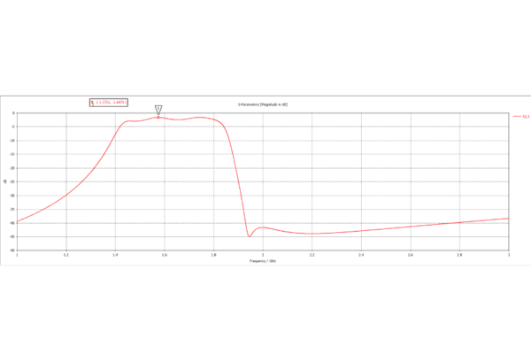
Vector Network Analyzer (VNA) Measurements
S-Parameters to Measure:
- S21 (Insertion Loss) - Power transmission through filter
- S11 (Return Loss) - Input impedance match
- S22 - Output impedance match
Typical Test Setup:
- Calibrate VNA (SOLT or TRL calibration)
- Mount DUT with appropriate fixtures
- Measure S-parameters over frequency range
- Compare to simulation/specification
Tuning Methods
For Prototypes:
- Add/remove copper with knife (lowpass/highpass)
- Add tuning screws for adjustable resonators
- Solder additional capacitors for fine tuning
For Production:
- Adjust design dimensions
- Optimize substrate thickness
- Change material if needed
- Re-simulate and verify
Applications
Wireless Communication
- Base station filters
- Mobile phone front-ends
- Wi-Fi and Bluetooth modules
- 5G millimeter-wave systems
Radar Systems
- Pulse compression filters
- Image rejection
- Harmonic filters
- Channel selection
Satellite Communication
- Transponder filters
- Up/down converter filtering
- Interference rejection
- Channel multiplexing
Test and Measurement
- Spectrum analyzer pre-selection
- Signal generator harmonics reduction
- EMI test equipment
- Calibration standards
Future Trends
Millimeter-Wave Filters
As 5G and satellite communications push into 28 GHz, 39 GHz, and beyond, microstrip filter design faces new challenges:
- Tighter manufacturing tolerances required
- Substrate losses more critical
- Radiation losses increase
- New materials needed
Integrated Passive Devices (IPD)
Combining microstrip with thin-film technology:
- Higher integration density
- Better performance
- Lower cost at volume
- Smaller size
AI and Machine Learning
The future of filter design:
- Automated topology selection
- Real-time optimization
- Predictive performance modeling
- Manufacturing compensation
Conclusion
Microstrip filter technology has evolved from simple printed circuits in 1952 to sophisticated electromagnetic structures enabling today’s wireless communications. The combination of:
- Advanced Materials - Low-loss, stable dielectrics
- Precise Manufacturing - Automated PCB processes
- Powerful Design Tools - Like RFOXiA’s AI-powered AFD
- Innovative Topologies - Compact, high-performance structures
…makes microstrip filters the technology of choice for most RF applications.
The RFOXiA AFD software represents the next generation of filter design tools, leveraging AI to automatically create optimized designs that minimize losses and maximize performance. By handling the complex electromagnetic calculations and optimization automatically, AFD makes professional-grade microstrip filter design accessible to engineers at all levels.
Whether you’re designing filters for 5G smartphones, satellite communications, or radar systems, microstrip technology combined with modern design tools provides the performance, size, and cost advantages needed for competitive products.
Ready to design your next microstrip filter? Contact RFOXiA to learn more about our AFD software and RF engineering services.